
JadeRover
-
Posts
154 -
Joined
-
Last visited
-
Days Won
2


JadeRover's Achievements
")


-

HP Elitebook 8570W - is it still good ? Hardware modifications
JadeRover replied to GuitarG's topic in Custom Builds
Correct, that's because there is no mux switch and non DC screen = LVDS lcd and the newest and fastest card that supports LVDS video signal is 980m. After maxwell generation Nvidia dropped support for LVDS. Therefore you would need a DC screen to upgrade to newer cards + backlight mods. Parts : - DC screen and cable - newer gpu - backlight cable mod Alternatively you can get someone to build a custom lcd cable to connect the lcd connector of the motherboard to any modern 30/40 pin edp display. Parts would be : - custom edp cable - standard laptop eDP display - new GPU - backlight mod cable Getting a custom edp cable has been done before, on taobao it is possible to order some custom ones based on the laptop lcd connector. -
HP Elitebook 8570W - is it still good ? Hardware modifications
JadeRover replied to GuitarG's topic in Custom Builds
Honestly no, we would need a board level rewiring to make the eDP from motherboard use DP_D position on mxm slot. Not viable in my opinion. What is viable however is to do a backlight mod, meaning you have to use an MXM gpu with regular DP (display port) on DP_C position. Then use a backlight v2 mod cable to get an image on the internal lcd. There's still a problem with windows drivers but that can be fixed as well. This is by far the best method and the mod cable is easy to install with no soldering. -
Quadro P4000 Mobile Oc vbios. Working and tested.
JadeRover replied to Ralph's topic in Components & Upgrades
@ssergey931 Yes that is because the iMac vbios has eDP on the correct spot for the zbook 17 g3. Other vbios have eDP signals on the wrong spot resulting in black screen if dGPU mode is selected. You can use my vbios overclocking program to get more performance out of it. I can get 1898Mhz on my core and 4504Mhz vram with my programs vbios. You feed it this iMac OC vbios and then select the clocks you want. The program only modifies clock tables, display tables are untouched and you will still be able to use the screen in dGPU mode. -
Nvidia-vBIOS-Clock-Power-Tweaker - PASCAL TESTING NEEDED !
JadeRover replied to JadeRover's topic in Components & Upgrades
Very nice, with an overclock you should get >1070M overclock levels of performance! Yes, I saw your post on techpowerup. It should work. If it doesn't send me your vbios and I will take a look. -
Nvidia-vBIOS-Clock-Power-Tweaker - PASCAL TESTING NEEDED !
JadeRover replied to JadeRover's topic in Components & Upgrades
Yes it happens with unsigned exes. You can download the source code, download python 3 and run CPR_MAIN.py and it will run the code directly without going through the packed exe. I see what you mean. The way the program works is by allowing the card to reach higher limit clocks. Meaning it will figure out the frequency/voltage points. It's not like msi afterburner's clock slider that uses the same voltage points but for higher clocks. For example, my p4000 stock vbios gave a maximum of 1240mhz @ 0.750v After the overclock from my program is applied it reaches 1898Mhz @1.050v. Unfortunately I doubt I will be able to obtain voltage control, I only found one person talking about voltage points and I could not find correlations with the clock table. -
(Potential) Fix for "pwr" limit of MXM GPU
JadeRover replied to JadeRover's topic in Components & Upgrades
Hi, Yes this is the same method as on this thread but the mod is done on the motherboard. Counting the pins on the second picture, pin 27 is actually the 9th pin after the big ground pad of MXM slot, so his method is also blocking the PWR_LVL signal from being sent to the MXM gpu. -
HP Elitebook 8570W - is it still good ? Hardware modifications
JadeRover replied to GuitarG's topic in Custom Builds
I checked again on the 8570w boardview and the LCD connector is wirred to DP_D of the MXM slot : Meaning no need for vbios mod I was wrong. If you have DC screen evey GPU with eDP support should work. What is the problem with 1070m @KbX ? no image ?
-
HP Elitebook 8570W - is it still good ? Hardware modifications
JadeRover replied to GuitarG's topic in Custom Builds
Unfortunately no, since non DC screen go through the LVDS port of the gpu and all pascal cards and above (including 1070m) don't have LVDS pins, no vbios can fix that. What it should do is make the 1070m work on DC screen since it wasn't possible before due to eDP placement mismatch in vbios. The 8570w doesn't use integrated graphics and the internal lcd goes directly to the dGPU if I am not mistaken. -
HP Elitebook 8570W - is it still good ? Hardware modifications
JadeRover replied to GuitarG's topic in Custom Builds
That is due to a vbios mismatch with the mxm slot regarding eDP placement on the 8570w. What he needs is a custom vbios that has eDP on DP_C position of the card as that's where it is located on the mxm slot of the laptop. Most laptops have eDP on position DP_D of the mxm slot so most vbios have it set to that. He can use this Macrumors vbios for 1070m that has eDP on DP_C (that luckily exists) : https://forums.macrumors.com/threads/imac-2011-maxwell-and-pascal-gpu-upgrade.2300989/page-10?post=30799977#post-30799977 I discovered this when my p3000 worked with the internal display of my zbook 17 g3 (eDP on position DP_C) once I used another "Mac compatible" vbios -
Nvidia-vBIOS-Clock-Power-Tweaker - PASCAL TESTING NEEDED !
JadeRover replied to JadeRover's topic in Components & Upgrades
V1.3.4 released. GitHub updated. Anyone with a pascal mobile card, a 1.8 volt firmware flasher like CH341a and spare time is welcome to use the program and try creating some custom vbioses. If you encounter issues I will ttake a look as to improve the program ! I can also use some testers for quadro P6 and P106m so that I can look into creating completely custom vbios for these cards. -
@Will Short answer : Yes and yes Yes, the dGPU will be used a a video accelerator selectable in windows. This allows even GPUs with no display outputs at all such as MXM gpus like the quadro tesla M6, P6, P106m, etc, to work in MXM based laptops Yes, I had put a P3000m in my zbook 17 g3 and I would get no dipslay out if I forced dGPU in the vbios, the reason being that zbook had eDP on DP_C and the card had eDP on DP_D. What I ended up doing was bridging the 3.3v and PNL_ON and PWM of the MXM slot and then forced the graphics mod to dGPU only in the vbios to get a video out. I then had a picture on the screen with no way to adjust brightness, it was stuck at 100%. Using an eDP cable mod v1 or v2 will be much simpler (and less stressful) than soldering direclty to the pins. HOWEVER, nvidia drivers will decide "screw that" after they install and will disconnect the dGPU from the screen, usually ~10 seconds after windows loads and the driver starts. SuperMG found a workaround in windows to force the screen to stay on after the drivers install luckily, it is detailed in his "eDP cable mod" PDF instrutions.
-
Nvidia-vBIOS-Clock-Power-Tweaker - PASCAL TESTING NEEDED !
JadeRover replied to JadeRover's topic in Components & Upgrades
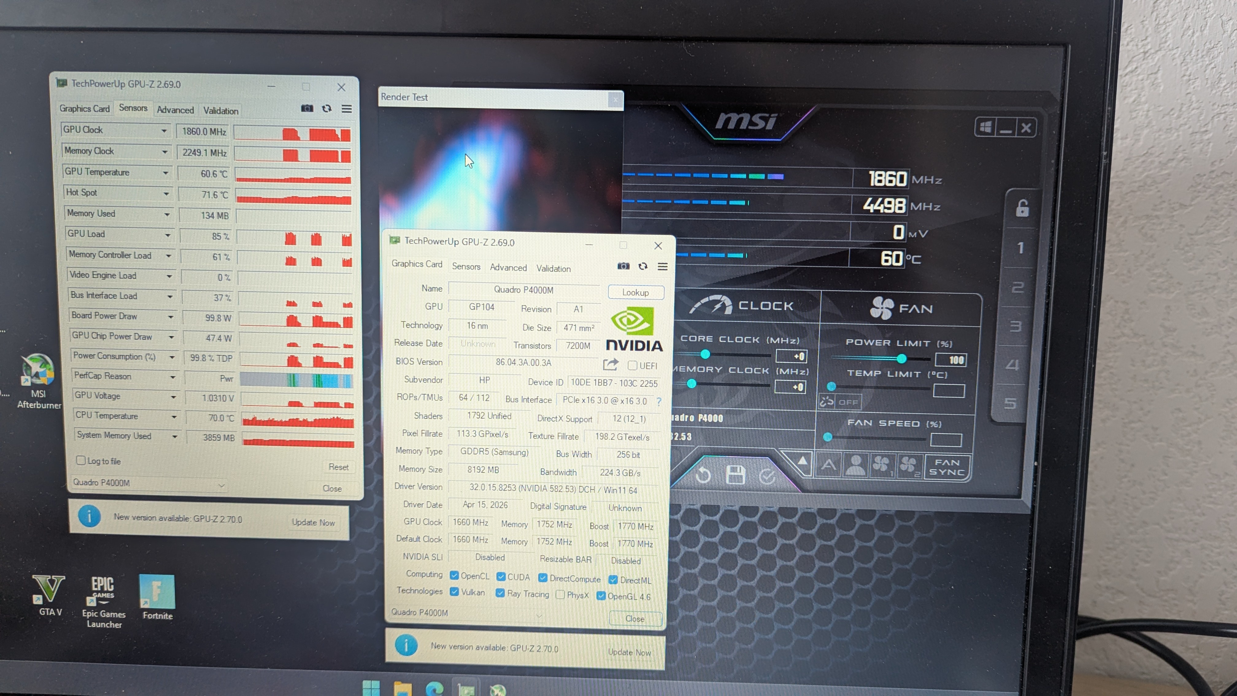
Hello everyone, Good news, an actual working version of the tool, v1.3.4 is in the works. The secret? Actually do some real life rigorous testing 😉 Here is some extreme overclocking on my p4000: That's right, compared to the base 1240mhz core and 3000mhz vram, we have a +800mhz core and +1500mhz on vram. Netting me a nice score (8th currently due to thermal throttle) : 3D mark p4000 leaderboard The tool should work with all pascal mxm modules. P1000 and P2000 are still in the works (not sure if I'll implement them) all others are functioning. Release coming soon.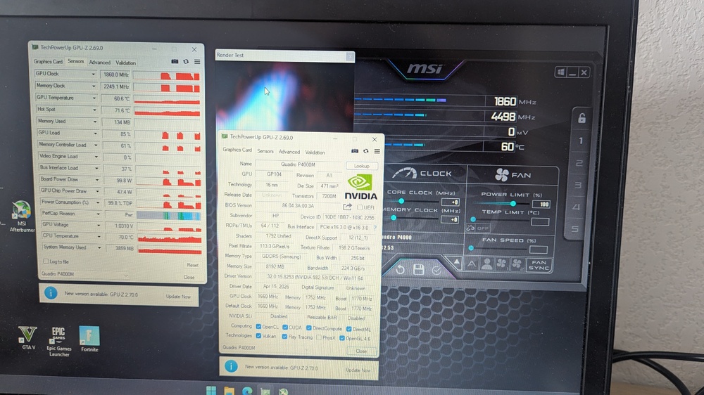
-
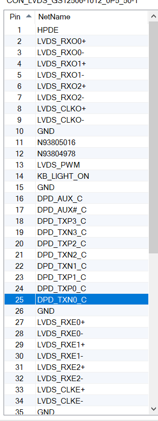
What’s the deal with eDP pin pitch adapters?
JadeRover replied to commanderf's topic in Components & Upgrades
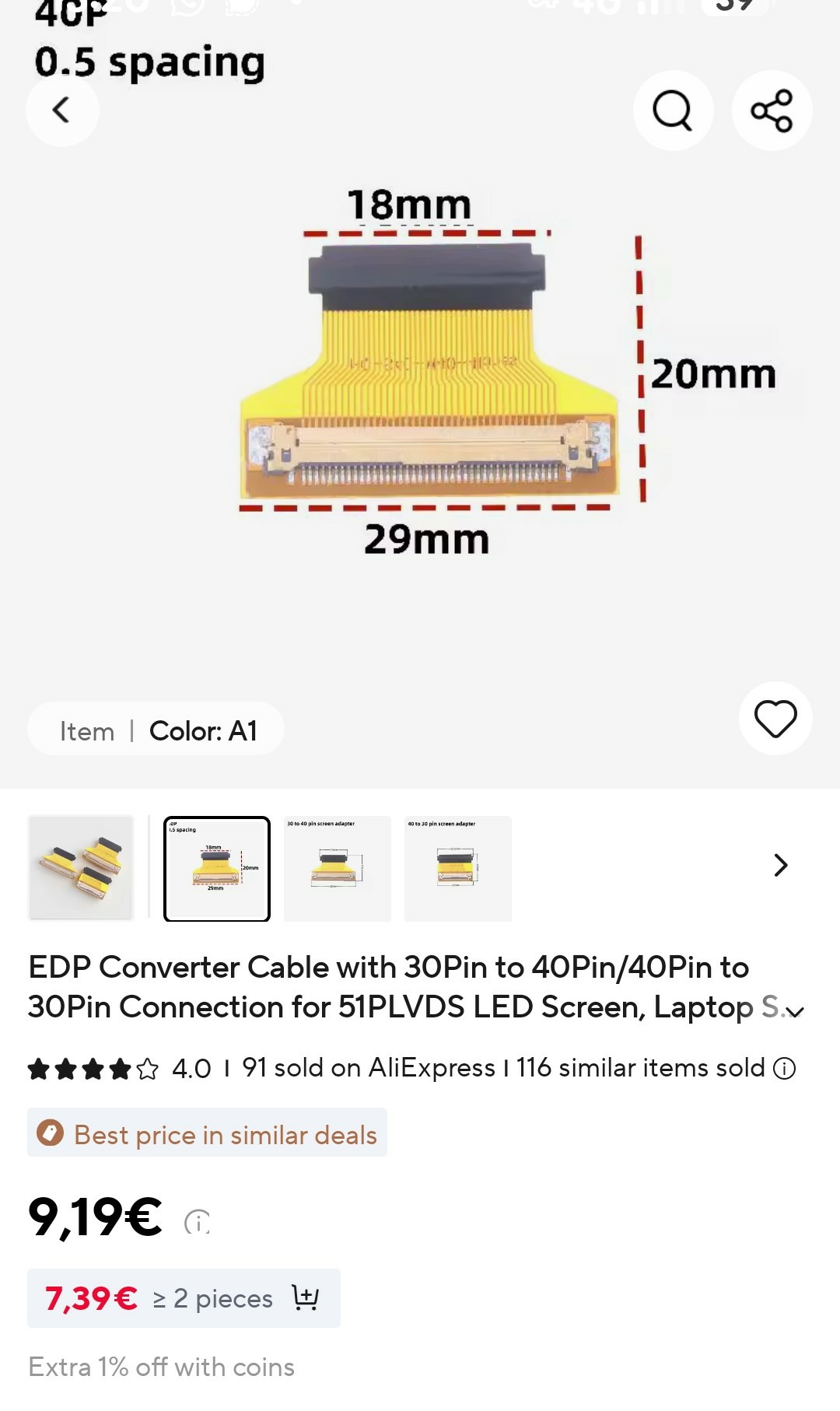
Hello, yes they make such flex cables that go from 40 pin .5 to 40 pin .4 I have used such an adapter for my precision 7720 to connect to a 4k .4 pitch lcd. They are a but flimsy and yes they have no retaining clips. However the sellers provide double sided tape. What you do is insert the male of the cable into the lcd (secure with tape so it won't move). Flip the flex cable around, remove sticky tape and stick it on the top of the lcd controller board. Voilà you converted your lcd to .5 pitch! Unfortunately I don't have any pictures of the installation. Here is one of the flex cable.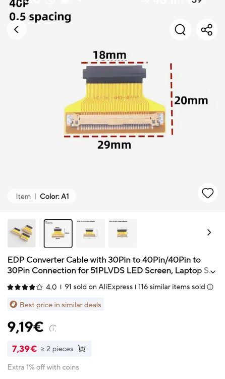
-
[6820hq Skylake] Precision 7720 extreme mods
JadeRover replied to JadeRover's topic in Components & Upgrades
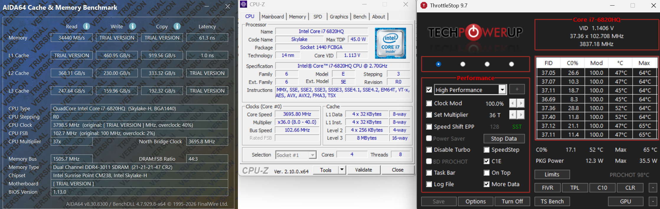
Hello, so a bit of an update I got 2x8gb of 3200Mhz ram at a good price, using smockeless UMAF I first booted into the "Advanced" bios with some 2666Mhz ram and limited Ram speed to 2933Mhz. If I booted directly with my 3200Mhz sticks, since the machine goes for the highest speed you ram can achieve, it will not boot at 3200Mhz and gives a ram error code. Doing this method allows me to then swap the 2666Mhz ram for my 2x8gb of 3200Mhz ram and here are the results with a 102.7Mhz BCLK ! That's right, thanks to BCLK overclocking my ram is now running at 3011Mhz ! 3Ghz barrier passed ! Also for skyake the PCIe and BCLK clocks are seperate, I went over the documentation again and that is why you can get high BCLK value without causing problems for the rest of the system (only ram and cpu get a clock boost). I still need to find a way to get more than 102.7Mhz that is limited by intel ME version. I know it is possible as in this review of the MSI GT83vr with 6920HQ cpu, they achieved close to 105Mhz bclk : Overclocking sur le PC portable MSI GT83VR 6RF-037FR (SLI GTX 1080 / Core i7-6920HQ) Zoom of the picture :
-
Hello, how is your project doing ? I am curious, did you isntall the xeon motherboard ? If so can you get throttlestop and check if the cpu has some overclocking bins ? I am curious if xeons have them as I am currently hesitating between getting a xeon motherboard or a 7920hq motherboard that I know for a fact has +6 turbo overclocking bins. Thanks.